Wafer Stepper: Difference between revisions
No edit summary |
|||
| Line 45: | Line 45: | ||
* Spectral Line: 365 nm wavelength (aka "i-line") via Hg lamp | * Spectral Line: 365 nm wavelength (aka "i-line") via Hg lamp | ||
* System is setup for 4 inch wafers and pieces smaller than 100mm. | * System is setup for 4 inch wafers and pieces smaller than 100mm. | ||
== Related Instrumentation in the KNI == | |||
===== Electron Beam Lithography ===== | |||
* [[EBPG 5200: 100 kV Electron Beam Lithography|EBPG 5200: 100 kV Electron Beam Lithography]] | |||
* [[EBPG 5000+: 100 kV Electron Beam Lithography | EBPG 5000+: 100 kV Electron Beam Lithography]] | |||
* [[Quanta 200F: SEM, ESEM, Lithography & Probe Station | Quanta 200F: SEM with 1-30 kV Electron Beam Lithography]] | |||
* [[Tecnai TF-20: 200 kV TEM, STEM, EDS, EELS, EFTEM & Lithography | Tecnai TF-20: TEM & STEM with 80-200 kV Electron Beam Lithography]] | |||
===== Ion Beam Lithography ===== | |||
* [[ORION NanoFab: Helium, Neon & Gallium FIB | ORION NanoFab: Helium (5-40 kV), Neon (5-35 kV) & Gallium (1-30 kV) Focused Ion Beam Lithography & Microscopy]] | |||
===== Optical Lithography ===== | |||
* [[Contact Mask Aligners: MA6 & MA6/BA6 | Contact Mask Aligners: Suss MicroTec models MA6 & MA6/BA6]] | |||
* [[CNI-PV 2.1: Nano Imprint Lithography | Nano Imprint Lithography: NILT CNI-PV 2.1]] | |||
* [[DWL-66: Direct-Write Laser System | Direct-Write Laser System: Heidelberg Instruments DWL-66]] | |||
* [[Nanoscribe PPGT: Microscale 3D Printer | Two-Photon Lithography (aka Microscale 3D Printing): Nanoscribe Photonic Professional GT]] | |||
* [[Optical Lithography Resources]] | |||
Revision as of 16:35, 12 October 2020
|
Description
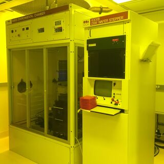
The 6000 Series DSW Wafer Stepper wafer exposure system is fully automatic and capable of exposing an array of images directly on photoresist-coated wafers. Image field size is dependent on the lens selected for the user's particular application. The lens in this system is a Zeiss 10X with a maximum field size of 10 mm x 10 mm. This reduces the pattern from the reticle by a factor of 10 onto the substrate. The KNI stepper has paddles for wafer handling to accommodate 2-, 3-, 4-, 6-, and 8-inch wafers as well as pieces. The stepper is located inside of an environmental chamber set to maintain +/-0.1 °C temperature control.
Software allows conversational input dialogue to reduce errors and simplify the specification of complex operating parameters, a part of which permits selection of either circular of rectangular arrays on the wafer. A laser position transducer with automatic compensation for atmospheric conditions and work piece temperature is employed to meter X- & Y-coordinate stage positioning over a 150 mm x 150 mm (6 in x 6 in) square exposable area. Maximum throughput is assured through use of X- & Y-coordinate stage speeds of up to 50 mm (2 in) per second and exposures in both directions of travel (boustrophedonic stepping). The GCA 6300 at KNI has been fully refurbished by RZE Enterprises with a new PC and control electronics.
Applications
- Step exposure with alignments
- Step exposure without alignments
Resources
Equipment Data
SOPs
Optical Lithography Resources
Manufacturer Manuals
- System Operation Manual
- Advanced Operation & Utilization Manual
- Advanced Information Package
- Reticle Handbook
- Baseline Procedure
- Acceptance Test Procedures
Specifications
- Spectral Line: 365 nm wavelength (aka "i-line") via Hg lamp
- System is setup for 4 inch wafers and pieces smaller than 100mm.
Related Instrumentation in the KNI
Electron Beam Lithography
- EBPG 5200: 100 kV Electron Beam Lithography
- EBPG 5000+: 100 kV Electron Beam Lithography
- Quanta 200F: SEM with 1-30 kV Electron Beam Lithography
- Tecnai TF-20: TEM & STEM with 80-200 kV Electron Beam Lithography
