Tecnai TF-20: 200 kV TEM, STEM, EDS, EELS, EFTEM & Lithography
|
Description
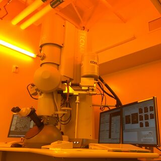
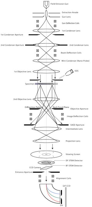
The Tecnai TF-20 is a transmission electron microscope (TEM) that can also be operated in scanning transmission electron microscopy (STEM) mode, with a voltage range of 40 to 200 kV. The TF-20 is equipped with bright field, dark field, and secondary electron detectors for use in STEM mode, an energy dispersive spectroscopy (EDS) detector for compositional analysis (in both TEM mode and, most often, in STEM mode), electron energy loss spectroscopy (EELS) & energy-filtered TEM (EFTEM), and a nanometer pattern generating system (NPGS) for performing lithography. Note that the KNI also has a 300 kV TEM, the Tecnai TF-30, which achieves higher resolution (albeit with fewer analytical options). See a full list of training and educational resources for this instrument below.
Applications
- High-Resolution TEM (HRTEM) imaging without an objective aperture
- Bright Field (BF) & Dark Field (DF) imaging with an objective aperture
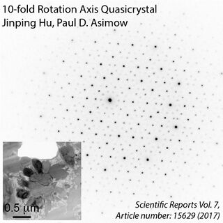
- Selected Area Electron Diffraction (SAED)
- STEM imaging with a BF, DF & Secondary Electron (SE) detector
- Energy Dispersive Spectroscopy (EDS) with an EDAX Genesis system
- Electron Energy Loss Spectroscopy (EELS) & Energy-Filtered TEM (EFTEM)
- E-beam lithography with Nanometer Pattern Generating System (NPGS) software
Resources
Equipment Data
SOPs & Troubleshooting
- SOPs (Long Version | Short, Conceptual Version)
- STEM mode EDS on TF-20 TEM (emphasis on high-resolution 2D mapping)
- Procedure to Evaluate Selected Area Electron Diffraction (SAED) Patterns
- Troubleshooting Guide
Manufacturer Resources
- Full manufacturer manual is accessible via the UI under the Help menu
Other Online Resources
- Rodenburg.org's Learn to Use a TEM
Sample Preparation
- Sample preparation is a highly specific task related to each sample type and is therefore primarily the responsibility of the user to carry out.
- KNI staff can teach users how to create lamellae from a bulk specimen using an SEM/Ga-FIB system (see SOP and YouTube playlist)
- The KNI also has a TEM sample preparation lab that is primarily used to make cross-section samples by traditional methods (i.e. glue together a stack, cut out 3 mm core, thin by polishing, dimple, then final polish with argon mill); inquire with staff for help with these sample preparation tools
Order Your Own Grids
- Grids used for mounting specimens are considered a personal, consumable item in the KNI. You are required to supply your own grids.
Specifications
Manufacturer Specifications
TEM & STEM Specifications
- From FEI’s (now Thermo Fisher’s) Tecnai G2 20 Family
- Voltage Range: 80-300 kV
- Point resolution: 0.27 nm
- Line resolution: 0.144 nm
- STEM resolution: 1.0 nm
- Information limit: 0.18 nm
- Energy spread: 0.7 eV
- Max alpha-tilt angle with double-tilt holder: ±50°
- Maximum diffraction angle: ±10°
- Camera length: 35–2300 mm
- EDS solid angle: 0.13 srad
Related Instrumentation in the KNI
Transmission Electron Microscopes
- Tecnai TF-30: TEM, STEM, EDS & HAADF (50-300 kV)
- Tecnai TF-20: TEM, STEM, EDS, EELS, EFTEM & Lithography (40-200 kV)
Sample Preparation for TEM
- Nova 600 NanoLab: SEM, Ga-FIB, GIS & Omniprobe
- TEM Sample Preparation Equipment: Polishing Stations, 3 mm Disk Cutter, Dimpler, Argon Ion Mill
Scanning Electron Microscopes (SEMs)
- Nova 600 NanoLab: SEM, Ga-FIB, GIS & Omniprobe
- Nova 200 NanoLab: SEM, EDS & WDS
- Sirion: SEM & EDS
- Quanta 200F: SEM, ESEM, Lithography & Probe Station


