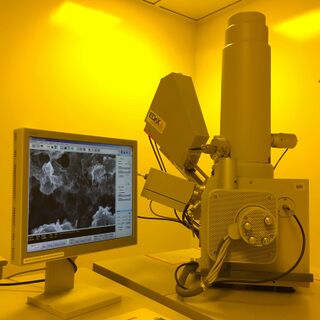
Sirion: SEM & EDS
Jump to navigation
Jump to search
|
Description
The Sirion is a field emission gun (FEG) scanning electron microscope (SEM) equipped with an immersion lens for imaging sub-10 nm features (so-called "ultra high resolution mode," UHR). While it is the KNI's oldest SEM, it is also a very steady instrument, offering a lower-cost alternative to similar high-resolution imaging that is available on the newer Nova 600 platform. The smaller Sirion chamber also allows for fast pump and vent times, which makes this SEM very useful for quick inspection. See a full list of training and educational resources for this instrument below.
SEM Applications
- Ultra-High-Resolution Imaging (Immersion Mode aka UHR Mode)
- High-Resolution Imaging (Field-Free Mode aka Normal Mode)
- Secondary Electron (SE) & Backscattered Electron (BSE) Imaging
- Everhart-Thornley Detector (ETD) & Through-the-Lens Detector (TLD)
Resources
SOPs & Troubleshooting
Video Tutorials
- Getting Started | Basic SEM Alignment
- Astigmatism Correction (Details | On Right-Angle Features | Stigmator Alignment)
- Adjusting TLD Voltage to Capture SE vs. BSE Signal
Graphical Handouts
Presentations
- Masterclasses for Microscopy
SEM Essentials: Capabilities and Limitations of Scanning Electron Microscopy; and SEM Setup, Parameters and Theory for Successful Operations and Measurements
- Scanning Electron Microscopy: Principles, Techniques & Applications
Calibrate Measurements with NIST Standard
- The KNI has a NIST-traceable standard against which SEM measurements can be compared. See Slides 54-55 of the SEM Presentation for details. Ask staff for help finding and using the standard in the lab.
Simulation Software
- CASINO Electron Beam Simulation Software – simulate e-beam/specimen interactions
Sample Preparation
- Use the Carbon Evaporator to make non-conductive samples conductive by applying 2-10 nm of evaporated carbon.
- Use the O2/Ar Plasma Cleaner to remove hydrocarbons from the sample surface to avoid creating dark contamination spots on your features while imaging them.
Stubs for specimen mounting
- Stubs used for mounting specimens are considered a personal, consumable item in the KNI. There are some stubs at each Microscope which can be used by any KNI microscopy user. You can also buy your own stubs so that you can keep them clean and available to you. There are many stub geometries and configurations. If you chose to buy your own stubs, please show them to the staff microscopist prior to using them: some stubs including stubs with copper clips have large height differences and can only be used safely in specific operating conditions.
Guide to Choosing KNI SEMs & FIBs
Specifications
Manufacturer Specifications
SEM Specifications
- Minimum Feature Size Resolved: ~7 nm
- Voltage Range: 0.2 to 30.0 kV
- Current Range: "Spotsize" 1 to 7 (approximately 30 pA to 20 nA), with increments of 1
- Apertures: 30 μm, 40 μm, 50 μm, 100 μm
- Eucentric Height: 5 mm working distance (WD)
- Stage Range: ±25 mm X & Y travel, 50 mm Z travel, 0-45° tilt, 360° rotation
- ETD Grid Bias Range: -150 to 300 V
- TLD Bias Range: -100 to 150 V
- Ultimate Vacuum: 3e-6 mbar
