ORION NanoFab: Helium, Neon & Gallium FIB: Difference between revisions
No edit summary |
No edit summary |
||
| Line 119: | Line 119: | ||
* Writing Speed: 20 MHz | * Writing Speed: 20 MHz | ||
* Digital-to-Analog Converter (DAC): 16-bit | * Digital-to-Analog Converter (DAC): 16-bit | ||
<br> | |||
<br> | |||
== Related Instrumentation in the KNI == | == Related Instrumentation in the KNI == | ||
===== Focused Ion Beam (FIB) Systems ===== | ===== Focused Ion Beam (FIB) Systems ===== | ||
| Line 132: | Line 133: | ||
* [[Carbon Evaporator | Carbon Evaporator (Leica EM ACE600) to make samples conductive]] | * [[Carbon Evaporator | Carbon Evaporator (Leica EM ACE600) to make samples conductive]] | ||
* [[Tergeo Plus ICP- & CCP-RIE: Oxygen & Argon Plasma Cleaner | Oxygen & Argon Plasma Cleaner (Tergeo Plus ICP- & CCP-RIE) to remove hydrocarbons from surface]] | * [[Tergeo Plus ICP- & CCP-RIE: Oxygen & Argon Plasma Cleaner | Oxygen & Argon Plasma Cleaner (Tergeo Plus ICP- & CCP-RIE) to remove hydrocarbons from surface]] | ||
===== Lithography ===== | |||
* [[EBPG 5200: 100 kV Electron Beam Lithography | EBPG 5200: Electron Beam Pattern Generator (100 kV)]] | |||
* [[EBPG 5000+: 100 kV Electron Beam Lithography | EBPG 5000+: Electron Beam Pattern Generator (100 kV)]] | |||
* [[Quanta 200F: SEM, ESEM, Lithography & Probe Station | Quanta 200F: SEM, ESEM, Lithography & Probe Station]] | |||
===== Transmission Electron Microscopes ===== | ===== Transmission Electron Microscopes ===== | ||
* [[Tecnai TF-30: 300 kV TEM, STEM, EDS & HAADF | Tecnai TF-30: TEM, STEM, EDS & HAADF (50-300 kV)]] | * [[Tecnai TF-30: 300 kV TEM, STEM, EDS & HAADF | Tecnai TF-30: TEM, STEM, EDS & HAADF (50-300 kV)]] | ||
Revision as of 22:43, 12 September 2019
|
Description
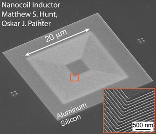
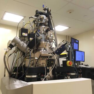
The ORION NanoFab is a focused ion beam (FIB) system capable of generating three different ion beams – helium & neon from the gas field ion source (GFIS) that is aligned on the main optical axis, and gallium offset by 54°, as in a more traditional "dual beam" FIB/SEM (scanning electron microscope). The He beam, which can be formed into a sub-0.5 nm probe size, is capable of high-resolution imaging, lithography and etching, with each performing in the sub-5 nm regime. The Ne beam, with a 1.9 nm probe size, can etch sub-15 nm features with order-of-magnitude higher volume-removal rates than He, and perform sub-10 nm lithography on resist. The Ga beam, with a 5 nm minimum probe size, can remove relatively large volumes of material by direct etching. In all, the three beams, each operating over large energy ranges (see specifications below for details), provide multitudes of nanofabrication opportunities in a single system.
Imaging Applications
- Ultra-High-Resolution imaging (capable of resolving sub-5 nm features)
- High depth of field imaging (compared to SEM)
- Image non-conductive specimens using an electron flood gun for charge compensation
Etching Applications
- Directly etch patterns into material with all three beams – He, Ne & Ga
- Cutting & Imaging Cross-Sections (using Ga)
- Final thinning of TEM lamellae (using Ne)
- Pattern with Raith ELPHY MultiBeam Pattern Generator or Nanometer Patterning & Visualization Engine (NPVE)
Lithography Applications
- High-resolution patterning on resist (35 keV He ions can perform better than 100 keV electrons)
- Automatic alignment to markers and automated processing (manually confirmed alignment also available)
- Resist patterning on non-conductive specimens
- Resist Pattering on curved substrates due to high depth of field
- Pattern with Raith ELPHY MultiBeam Pattern Generator or Nanometer Patterning & Visualization Engine (NPVE)
Resources
SOPs & Troubleshooting
- SOP for Basic Operation of ORION NanoFab
- SOP for Operating Raith ELPHY MultiBeam Pattern Generator
- Troubleshooting Guide
Video Tutorials
- Getting Started | Introduction to GFIS Parameters (He- & Ne-FIB)
- GFIS Alignments (He- & Ne-FIB)
- Using the Electron Flood Gun for Charge Compensation
- Eucentric Height: What it means, When to use it & How to get there (recorded for SEM, same principles apply here)
- Cutting & Imaging Cross-sections (Playlist) (recorded on SEM/Ga-FIB)
- Preparing a Trimer (Playlist)
Graphical Handouts
Presentations
- Helium & Neon Focused Ion Beam Microscopy: Principles, Techniques & Applications
- Gallium Focused Ion Beam Microscopy: Principles, Techniques & Applications
Manufacturer Manuals
- Zeiss ORION NanoFab Operation Manual
- Raith ELPHY MultiBeam: Software Operation Manual | Software Reference Manual |Step-by-Step Patterning Guide
- Nanometer Patterning & Visualization Engine (NPVE) Operation Manual
Simulation Software
- The Stopping & Range of Ions in Matter (SRIM) – simulate i-beam/specimen interactions
- CASINO Electron Beam Simulation Software – simulate e-beam/specimen interactions
Calibrate Measurements with NIST Standard
- The KNI has a NIST-traceable standard against which FIB measurements can be compared. See Slides 54-55 of the SEM Presentation for details. Ask staff for help finding and using the standard in the lab.
Sample Preparation
- Use the Carbon Evaporator to make non-conductive samples conductive by applying 2-10 nm of evaporated carbon (first try using the in-chamber electron flood gun to alleviate charge artifacts).
- Use the O2/Ar Plasma Cleaner to remove hydrocarbons from the sample surface to avoid creating dark contamination spots on your features while imaging them (the ORION's in-chamber plasma cleaner can be used in extreme cases where the sample must be cleaned directly before the experiment is conducted, without exposing it to the atmosphere while transferring it from the outside cleaner to the ORION chamber; excessive numbers of chamber cleanings can have adverse effects on the ORION over time so consult with staff on how and when to do this).
Order Your Own Stubs
- Stubs used for mounting specimens are considered a personal, consumable item in the KNI. There are some old stubs at each SEM & FIB, yet you should buy your own so that you can keep them clean and available to you. There are many stub geometries and configurations, some of which will be right for you to purchase and keep with your other cleanroom items.
- Buy stubs with copper clips (recommended for most devices, esp with non-conductive substrates);
- Buy stubs without copper clips (ok for devices with conductive substrates)
Specifications
Manufacturer Specifications
Overall System Specifications
- Eucentric Height: ~9.1 mm working distance (WD)
- Allowable Sample Width: 80 mm (this is the width of the load lock opening)
- Stage Range: ±24 mm X & Y travel, 8 mm Z travel, -10 to 58° tilt, 360° rotation
- ETD Grid Bias Range: -250 to 250 V
- Stage Bias Range: -500 to 500 V
- Ultimate Vacuum: 2e-7 Torr
He-FIB Specifications
- Minimum Feature Size Resolved with He Imaging: ~3 nm
- Minumum Probe Size: 0.35 nm
- Voltage Range: 5 to 40 kV
- Current Range: 0.1 to 100 pA
Ne-FIB Specifications
- Minimum Feature Size Resolved with Ne Imaging: ~7 nm
- Minumum Probe Size: 1.9 nm
- Voltage Range: 5 to 35 kV
- Current Range: 0.1 to 50 pA
Ga-FIB Specifications
- Minimum Feature Size Resolved with Ga Imaging: ~10 nm
- Minumum Probe Size: 3 nm
- Voltage Range: 1 to 30 kV
- Current Range: 1 pA to 100 nA
Electron Flood Gun Specifications
- Probe Diameter: millimeters (can be roughly focused)
- Voltage Range: 0.025 to 1.0 kV
- Current: ~1 μA
- Dwell Time Range: 50 to 10000 μs
Raith ELPHY MultiBeam Specifications
- Shapes Available: Polygons (area dose), Single Pass Lines (line dose) & Dot Arrays (point dose) of any arbitrary shape
- Import CAD files as .dxf or .gds files
- Writing Speed: 20 MHz
- Digital-to-Analog Converter (DAC): 16-bit
Related Instrumentation in the KNI
Focused Ion Beam (FIB) Systems
Scanning Electron Microscopes (SEMs)
- Nova 600 NanoLab: SEM, Ga-FIB, GIS & Omniprobe
- Nova 200 NanoLab: SEM, EDS & WDS
- Sirion: SEM & EDS
- Quanta 200F: SEM, ESEM, Lithography & Probe Station
Sample Preparation for Microscopy
- Carbon Evaporator (Leica EM ACE600) to make samples conductive
- Oxygen & Argon Plasma Cleaner (Tergeo Plus ICP- & CCP-RIE) to remove hydrocarbons from surface
Lithography
- EBPG 5200: Electron Beam Pattern Generator (100 kV)
- EBPG 5000+: Electron Beam Pattern Generator (100 kV)
- Quanta 200F: SEM, ESEM, Lithography & Probe Station
Transmission Electron Microscopes
- Tecnai TF-30: TEM, STEM, EDS & HAADF (50-300 kV)
- Tecnai TF-20: TEM, STEM, EDS, EELS, EFTEM & Lithography (40-200 kV)

