Sirion: SEM & EDS: Difference between revisions
Jump to navigation
Jump to search
No edit summary |
No edit summary |
||
| Line 88: | Line 88: | ||
* [[Carbon Evaporator | Carbon Evaporator (Leica EM ACE600) to make samples conductive]] | * [[Carbon Evaporator | Carbon Evaporator (Leica EM ACE600) to make samples conductive]] | ||
* [[Tergeo Plus ICP- & CCP-RIE: Oxygen & Argon Plasma Cleaner | Oxygen & Argon Plasma Cleaner (Tergeo Plus ICP- & CCP-RIE) to remove hydrocarbons from surface]] | * [[Tergeo Plus ICP- & CCP-RIE: Oxygen & Argon Plasma Cleaner | Oxygen & Argon Plasma Cleaner (Tergeo Plus ICP- & CCP-RIE) to remove hydrocarbons from surface]] | ||
===== Transmission Electron Microscopes ===== | |||
* [[Tecnai TF-30: 300 kV TEM, STEM, EDS & HAADF | Tecnai TF-30: TEM, STEM, EDS & HAADF (50-300 kV)]] | |||
* [[Tecnai TF-20: 200 kV TEM, STEM, EDS, EELS, EFTEM & Lithography | Tecnai TF-20: TEM, STEM, EDS, EELS, EFTEM & Lithography (40-200 kV)]] | |||
===== Scanning Probe Microscopes ===== | |||
* [[Dimension Icon: Atomic Force Microscope (AFM) | Dimension Icon: Atomic Force Microscope (AFM)]] | |||
* [[Dektak 3ST: Profilometer | Dektak 3ST: Profilometer]] | |||
Revision as of 23:53, 11 September 2019
|
Description
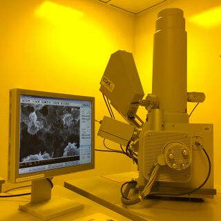
The Sirion is a field emission gun (FEG) scanning electron microscope (SEM) equipped with an immersion lens for imaging sub-10 nm features (so-called "ultra high resolution mode," UHR) and an energy dispersive spectroscopy (EDS) detector for compositional analysis. While it is the KNI's oldest SEM, it is also a very steady instrument, offering a lower-cost alternative to similar high-resolution imaging that is available on the newer Nova 600 & Nova 200 NanoLab platforms. The smaller Sirion chamber also allows for fast pump and vent times, which makes this SEM very useful for quick inspection. See a full list of training and educational resources for this instrument below.
SEM Applications
- Ultra-High-Resolution Imaging (Immersion Mode aka UHR Mode)
- High-Resolution Imaging (Field-Free Mode aka Normal Mode)
- EDX Mode Imaging (reduces background signal on EDS spectra)
- Secondary Electron (SE) & Backscattered Electron (BSE) Imaging
- Everhart-Thornley Detector (ETD) & Through-the-Lens Detector (TLD)
EDS Applications
- Spectrum acquisition for quantitative compositional analysis
- Linescan acquisition for 1D spatial compositional analysis
- Map acquisition for 2D spatial compositional analysis
Resources
SOPs & Troubleshooting
- SEM SOPs (Short Version | Long Version)
- EDS SOPs (Short Version | Long Version)
- Troubleshooting Guide
Video Tutorials
- Getting Started | Basic SEM Alignment
- Astigmatism Correction (Details | On Right-Angle Features | Stigmator Alignment)
- Eucentric Height: What it means, When to use it & How to get there
- Adjusting TLD Voltage to Capture SE vs. BSE Signal
Graphical Handouts
Presentations
- Scanning Electron Microscopy: Principles, Techniques & Applications (includes slides on EDS)
Manufacturer Manuals
Calibrate Measurements with NIST Standard
- The KNI has a NIST-traceable standard against which SEM measurements can be compared. See Slides 54-55 of the SEM Presentation for details. Ask staff for help finding and using the standard in the lab.
Simulation Software
- CASINO Electron Beam Simulation Software – simulate e-beam/specimen interactions (very useful for EDS)
Sample Preparation
- Use the Carbon Evaporator to make non-conductive samples conductive by applying 2-10 nm of evaporated carbon.
- Use the O2/Ar Plasma Cleaner to remove hydrocarbons from the sample surface to avoid creating dark contamination spots on your features while imaging them.
Order Your Own Stubs
- Stubs used for mounting specimens are considered a personal, consumable item in the KNI. There are some old stubs at each SEM, yet you should buy your own so that you can keep them clean and available to you. There are many stub geometries and configurations, some of which will be right for you to purchase and keep with your other cleanroom items.
- Buy stubs with copper clips (recommended for most devices, especially those with non-conductive substrates)
- Buy stubs without copper clips (OK for devices with conductive substrates)
Specifications
Manufacturer Specifications
SEM Specifications
- Minimum Feature Size Resolved: ~7 nm
- Voltage Range: 0.2 to 30.0 kV
- Current Range: "Spotsize" 1 to 7 (approximately 30 pA to 20 nA), with increments of 1
- Apertures: 30 μm, 40 μm, 50 μm, 100 μm
- Eucentric Height: 5 mm working distance (WD)
- Stage Range: ±25 mm X & Y travel, 50 mm Z travel, 0-45° tilt, 360° rotation
- ETD Grid Bias Range: -150 to 300 V
- TLD Bias Range: -100 to 150 V
- Ultimate Vacuum: 3e-6 mbar
Related Instrumentation in the KNI
Scanning Electron Microscopes (SEMs)
- Nova 600 NanoLab: SEM, Ga-FIB, GIS & Omniprobe
- Nova 200 NanoLab: SEM, EDS & WDS
- Sirion: SEM & EDS
- Quanta 200F: SEM, ESEM, Lithography & Probe Station
Focused Ion Beam (FIB) Systems
Sample Preparation for Microscopy
- Carbon Evaporator (Leica EM ACE600) to make samples conductive
- Oxygen & Argon Plasma Cleaner (Tergeo Plus ICP- & CCP-RIE) to remove hydrocarbons from surface
Transmission Electron Microscopes
- Tecnai TF-30: TEM, STEM, EDS & HAADF (50-300 kV)
- Tecnai TF-20: TEM, STEM, EDS, EELS, EFTEM & Lithography (40-200 kV)
