Nova 600 NanoLab: SEM, Ga-FIB, GIS & Omniprobe: Difference between revisions
Jump to navigation
Jump to search
| Line 39: | Line 39: | ||
* Ga-FIB SOPs ([https://caltech.box.com/s/8uch8ygjmesmjtdfy65xth47izib0prg Short Version] | [https://caltech.box.com/s/grg6j3rob7c4ciblom1tdshklq62oxqp Long Version]) | * Ga-FIB SOPs ([https://caltech.box.com/s/8uch8ygjmesmjtdfy65xth47izib0prg Short Version] | [https://caltech.box.com/s/grg6j3rob7c4ciblom1tdshklq62oxqp Long Version]) | ||
* TEM Lamella Sample Preparation SOPs ([https://caltech.box.com/s/3l3w507dxwosuya3nbxgk30tdqyp4qy9 Short Version] | [https://caltech.box.com/s/pgioaribs7oj8r7g5nncmjjee2uyez2d Long Version]) | * TEM Lamella Sample Preparation SOPs ([https://caltech.box.com/s/3l3w507dxwosuya3nbxgk30tdqyp4qy9 Short Version] | [https://caltech.box.com/s/pgioaribs7oj8r7g5nncmjjee2uyez2d Long Version]) | ||
** [https://caltech.box.com/s/lhaweqbefmep8n79u4nvynsv0cjctuc1 Process Recipe for TEM Lamella prep for Thin Films on Si Substrates] | |||
* [https://caltech.box.com/s/1nmp75l3166vj9t1vwwpwu2zyfc4j6ol Cutting & Imaging Cross-Sections SOP] | * [https://caltech.box.com/s/1nmp75l3166vj9t1vwwpwu2zyfc4j6ol Cutting & Imaging Cross-Sections SOP] | ||
* [https://caltech.box.com/s/sz9pai0icsntnef6me23veiwtwdui0gm Troubleshooting Guide] | * [https://caltech.box.com/s/sz9pai0icsntnef6me23veiwtwdui0gm Troubleshooting Guide] | ||
| Line 69: | Line 70: | ||
* [https://caltech.box.com/s/j0t3w6i53jhfjcva8i4qvlatdh7t1tzw Gas Injection Systems – Deposition of Platinum (Technical Note)] | * [https://caltech.box.com/s/j0t3w6i53jhfjcva8i4qvlatdh7t1tzw Gas Injection Systems – Deposition of Platinum (Technical Note)] | ||
* [https://caltech.box.com/s/sm7q7teh5fo5hg3e6flkjbcbycmarrm3 Gas Injection Systems – Deposition of SiOx (Technical Note)] | * [https://caltech.box.com/s/sm7q7teh5fo5hg3e6flkjbcbycmarrm3 Gas Injection Systems – Deposition of SiOx (Technical Note)] | ||
* [https://caltech.box.com/s/4pcym0l9j1e8t9b2vznrzps9uk7b85mh Gas Injection Systems – Etching with IEE aka | * [https://caltech.box.com/s/4pcym0l9j1e8t9b2vznrzps9uk7b85mh Gas Injection Systems – Etching with IEE aka XeF<sub>2</sub> Etch (Technical Note)] | ||
* [https://caltech.box.com/s/b95pg59k003i9vn8y9elzem0tnxqg3fb Gas Injection Systems – Beam Chemistries Presentation] | * [https://caltech.box.com/s/b95pg59k003i9vn8y9elzem0tnxqg3fb Gas Injection Systems – Beam Chemistries Presentation] | ||
* [https://caltech.box.com/s/110tb0o8avjziwa1y4d017dbbcpkxfop Scripting – AutoScript Language Manual (year 2000 Technical Note: most complete)] | * [https://caltech.box.com/s/110tb0o8avjziwa1y4d017dbbcpkxfop Scripting – AutoScript Language Manual (year 2000 Technical Note: most complete)] | ||
Revision as of 04:20, 17 February 2020
|
Description
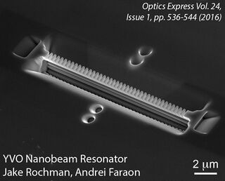
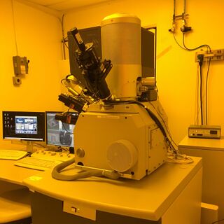
The Nova 600 is a "dual-beam" system that combines a field emission gun (FEG) scanning electron microscope (SEM) with a gallium focused ion beam (Ga-FIB). It can be used to capture high-quality images (clearly resolving sub-10 nm features) and perform site-specific etching and material deposition (creating sub-20 nm features). It is also equipped with an Omniprobe nanomanipulator, which can be used to lift out lamella samples that are prepared for use in a transmission electron microscope (TEM). See a full list of training and educational resources for this instrument below.
SEM Applications
- Ultra-High-Resolution Imaging (Immersion Mode aka UHR Mode)
- High-Resolution Imaging (Field-Free Mode aka Normal Mode)
- Secondary Electron (SE) imaging with an Everhart-Thornley Detector (ETD) & Through-the-Lens Detector (TLD)
- Backscattered Electron (BSE) imaging with a TLD
- Platinum deposition via Gas Injection System (GIS)
- Automated imaging with RunScript program & AutoScript language
Ga-FIB Applications
- Directly etch patterns into material
- Cutting & Imaging Cross-Sections
- TEM Lamella Sample Preparation using an Omniprobe for Liftout
- Platinum & SiOx deposition via GIS
- Enhanced etch with XeF2 via GIS
- Automated patterning with RunScript program & AutoScript language
Resources
SOPs & Troubleshooting
- SEM SOPs (Short Version | Long Version)
- Ga-FIB SOPs (Short Version | Long Version)
- TEM Lamella Sample Preparation SOPs (Short Version | Long Version)
- Cutting & Imaging Cross-Sections SOP
- Troubleshooting Guide
Video Tutorials
- Getting Started | Basic SEM Alignment
- Astigmatism Correction (Details | On Right-Angle Features | Stigmator Alignment)
- Eucentric Height: What it means, When to use it & How to get there
- Introduction to Using a Ga-FIB
- TEM Lamella Sample Prep (Playlist)
- Cutting & Imaging Cross-sections (Playlist)
- Milling Non-Conductive Samples using Charge Compensation
- Perfecting Ga-FIB Alignments
- Adjusting TLD Voltage to Capture SE vs. BSE Signal
Graphical Handouts
Presentations
- Scanning Electron Microscopy (SEM): Principles, Techniques & Applications
- Gallium Focused Ion Beam (Ga-FIB) Microscopy: Principles, Techniques & Applications
Manufacturer Manuals
- Nova NanoLab Operation Manual
- EDAX Genesis EDS & WDS Operation Manual
- Gas Injection Systems – Deposition of Platinum (Technical Note)
- Gas Injection Systems – Deposition of SiOx (Technical Note)
- Gas Injection Systems – Etching with IEE aka XeF2 Etch (Technical Note)
- Gas Injection Systems – Beam Chemistries Presentation
- Scripting – AutoScript Language Manual (year 2000 Technical Note: most complete)
- Scripting – AutoScript Language Manual (year 2005 Technical Note: less complete, still useful)
- Scripting – RunScript Manual
Simulation Software
- CASINO Electron Beam Simulation Software – simulate e-beam/specimen interactions
- The Stopping & Range of Ions in Matter (SRIM) – simulate i-beam/specimen interactions
Calibrate Measurements with NIST Standard
- The KNI has a NIST-traceable standard against which SEM and Ga-FIB measurements can be compared. See Slides 54-55 of the SEM Presentation for details. Ask staff for help finding and using the standard in the lab.
Sample Preparation
- Use the Carbon Evaporator to make non-conductive samples conductive by applying 2-10 nm of evaporated carbon.
- Use the O2/Ar Plasma Cleaner to remove hydrocarbons from the sample surface to avoid creating dark contamination spots on your features while imaging them.
Order Your Own Stubs
- Stubs used for mounting specimens are considered a personal, consumable item in the KNI. There are some old stubs at each SEM/FIB, yet you should buy your own so that you can keep them clean and available to you. There are many stub geometries and configurations, some of which will be right for you to purchase and keep with your other cleanroom items.
- Buy stubs with copper clips (recommended for most devices, esp with non-conductive substrates);
- Buy stubs without copper clips (ok for devices with conductive substrates)
Guide to Choosing KNI SEMs & FIBs
Specifications
Manufacturer Specifications
- Nova 600 NanoLab Data Sheet (not all parameters apply to our instrument, see below for details specific to the KNI's Nova 600)
SEM Specifications
- Minimum Feature Size Resolved in Immersion Mode: ~5 nm
- Voltage Range: 0.2 to 30.0 kV
- Current Range: ~10 pA to 20 nA
- Apertures: 10 μm, 15 μm, 20 μm, 30 μm
- Eucentric Height: ~5.15 mm working distance (WD)
- Stage Range: ±80 mm X & Y travel, 12 mm Z travel, -12 to 58° tilt, 360° rotation
- ETD Grid Bias Range: -150 to 300 V
- TLD Bias Range: -100 to 150 V
- Ultimate Vacuum: 5e-7 mbar
Ga-FIB Specifications
- Minumum Probe Size Achieved: ~7 nm
- Minimum Feature Size Etched: ~25 nm
- Minimum Feature Size Resolved by Imaging: ~10 nm
- Voltage Range: 5 to 30 kV
- Current Range: 1 pA to 20 nA
- Eucentric Height: ~5.15 mm working distance (WD)
- Stage Tilt to be perpendicular to Ga-FIB: 52°
- ETD Grid Bias Range: -150 to 300 V
- TLD Bias Range: -100 to 150 V
Related Instrumentation in the KNI
Scanning Electron Microscopes (SEMs)
- Nova 600 NanoLab: SEM, Ga-FIB, GIS & Omniprobe
- Nova 200 NanoLab: SEM, EDS & WDS
- Sirion: SEM & EDS
- Quanta 200F: SEM, ESEM, Lithography & Probe Station
Focused Ion Beam (FIB) Systems
Sample Preparation for Microscopy
- Carbon Evaporator (Leica EM ACE600) to make samples conductive
- Oxygen & Argon Plasma Cleaner (Tergeo Plus ICP- & CCP-RIE) to remove hydrocarbons from surface
Transmission Electron Microscopes
- Tecnai TF-30: TEM, STEM, EDS & HAADF (50-300 kV)
- Tecnai TF-20: TEM, STEM, EDS, EELS, EFTEM & Lithography (40-200 kV)

