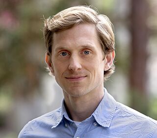
Matthew S. Hunt, PhD
|
About
Role in the KNI
Matthew Hunt was the Assistant Director of Staff Research and Lead Microscopist for The Kavli Nanoscience Institute (KNI) at the California Institute of Technology. He directed research projects that were carried out by KNI technical staff, in collaboration with Caltech & non-Caltech PIs and student researchers, with the purpose of creating new nanofabrication techniques using the KNI's leading edge instrumentation. He led the scientific side of the KNI SURF-the-WAVE Fellowships Program, which offers summer fellowships to non-Caltech undergraduate researchers, and also led the Lab Resident Expert Program, which provided top lab users an opportunity to give back to the lab in the form of process recipe development and new ideas for general lab improvement. Matt also managed and trained users on the KNI's suite of microscopy equipment: transmission electron microscopes, scanning electron microscopes, focused ion beam systems, an atomic force microscope, and related sample preparation equipment.
Matt joined the KNI in 2014 after completing his PhD related to the high temperature oxidation of turbine engine materials, through which he developed expertise in a number of electron, ion and x-ray microscopy techniques. His research interests lie in the development of new lithography and microscopy techniques that utilize various beam species (e.g. helium ions, neon ions, gallium ions, electrons) and the application thereof to the kinds of novel materials and devices that are important to users of the KNI.
Education
Matt received his Ph.D. and M.S. in Materials Science & Engineering from the University of California, Irvine and a B.S. in Chemical Engineering from the University of Notre Dame.
Lecture Materials

Microscopy Presentations
- Scanning Electron Microscopy: Principles, Techniques & Applications | YouTube Lecture
- Gallium Focused Ion Beam Microscopy: Principles, Techniques & Applications | YouTube Lecture
- Helium & Neon Focused Ion Beam Microscopy: Principles, Techniques & Applications | YouTube Lecture
Video Demonstrations
- SEM & Ga-FIB Alignments (Playlist)
- SEM & Ga-FIB Techniques (Playlist)
- Cutting & Imaging Cross-Sections (Playlist)
- TEM Lamella Sample Preparation with SEM/Ga-FIB (Playlist)
- Helium & Neon Ion Microscopy Alignments & Techniques (Playlist)
- Preparing a gas field ion source (GFIS) trimer for He- & Ne-FIB (Playlist)
- Introduction to AFM (Playlist)
Selected Publications
Articles

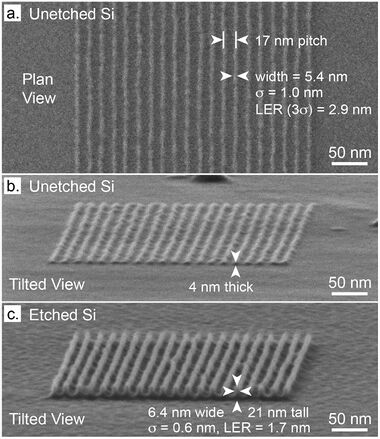
- Scott M. Lewis, Matthew S. Hunt, Guy A. DeRose, Hayden R. Alty, Jarvis Li, Alex Wertheim, Lucia De Rose, Grigore A. Timco, Axel Scherer, Stephen G. Yeates, and Richard E. P. Winpenny, "Plasma-Etched Pattern Transfer of Sub-10 nm Structures Using a Metal–Organic Resist and Helium Ion Beam Lithography," ACS Nano Letters 2019, available online: https://pubs.acs.org/doi/10.1021/acs.nanolett.9b01911.
- Scott M. Lewis, Guy A. DeRose, Matthew S. Hunt, Hayden Alty, Alex Wertheim, Jarvis Li, Trevor Fowler, Axel Scherer, Stepen G. Yeates, Richard E. P. Winpenny et al, "Design and Implementation of the Next Generation Electron Beam Resists for the Production of EUVL Photomasks," Photomask Technology 2018, p 24. https://doi.org/10.1117/12.2501808.
- Scott M. Lewis, Antonio Fernandez, Guy A. DeRose, Matthew S. Hunt, Axel Scherer, Stephen G. Yeates, Richard E. P. Winpenny et al, "Use of Supramolecular Assemblies as Lithographic Resists," Angew. Chem. Int. Ed. 2017, 56 (24), 6749–6752. https://doi.org/10.1002/anie.201700224.
- Matthew (Sullivan) Hunt, Daniel R. Mumm, "Transient stage oxidation of MCrAlY bond coat alloys in high temperature, high water vapor content environments," Surface and Coatings Technology 2014, Vol 258, 963-972. https://doi.org/10.1016/j.surfcoat.2014.07.048
- Matthew (Sullivan) Hunt, Daniel R. Mumm, "Vapor-Phase-Mediated Phenomena Associated with High Temperature, High Water Content Oxidation of MCrAlX Bond Coats," Oxidation of Metals 2014, Vol 82. 1. https://doi.org/10.1007/s11085-014-9473-8
Conference Presentations
- "Plasma-Etched Pattern Transfer of Sub-10 nm Structures Using a Metal–Organic Resist and Helium Ion Beam Lithography," Matthew S. Hunt, Guy A. DeRose, Hayden R. Alty, Alex Wertheim, Nathan S. Lee, Stephen G. Yeates, Richard E. P. Winpenny, Axel Scherer, and Scott M. Lewis. Presented at the EIPBN Conference in Minneapolis, MN on July 31, 2019.
- "Helium and Neon Focused Ion Beam Hard Mask Lithography on Atomic Layer Deposition Films," Matthew S. Hunt, Joshua Yang, Steven Wood, Nathan S. Lee, and Oskar J. Painter. Presented at the AVS Conference in Long Beach, CA on October 25, 2018.
List of Managed Instruments
Microscopy & Lithography
- Helium, Neon & Gallium FIB: Zeiss ORION NanoFab
- SEM, Ga-FIB, GIS & Omniprobe: Thermo Fisher Nova 600 NanoLab
- SEM, EDS & WDS: Thermo Fisher Nova 200 NanoLab
- SEM & EDS: Thermo Fisher Sirion
- SEM, ESEM, Lithography & Probe Station: Thermo Fisher Quanta 200F
- TEM, STEM, EDS & HAADF: Thermo Fisher Tecnai TF-30 (80-300 kV)
- TEM, STEM, EDS, EELS, EFTEM & Lithography: Thermo Fisher Tecnai TF-20 (80-200 kV)
- Atomic Force Microscope (AFM): Bruker Dimension ICON
- Fluorescence Microscope: Olympus IX81
