Nova 200 NanoLab: SEM & EDS: Difference between revisions
Jump to navigation
Jump to search
| Line 37: | Line 37: | ||
* [https://caltech.box.com/s/mpsxkxmf5y8wjw9daijwbudeoqkkeudu KNI Microscopy Policies] | * [https://caltech.box.com/s/mpsxkxmf5y8wjw9daijwbudeoqkkeudu KNI Microscopy Policies] | ||
* [https://caltech.box.com/s/4f1hqp83pwc1v1k5qke6xi68i28fjvz8 Nova200 and EDS SOP, Manuals, SDS] | * [https://caltech.box.com/s/4f1hqp83pwc1v1k5qke6xi68i28fjvz8 Nova200 and EDS SOP, Manuals, SDS] | ||
* [https://caltech.box.com/s/og4309108q4k2jwhkaxqtpiujg2al5iu Nova NanoLab Operation Manual] | |||
* [https://caltech.box.com/s/fime6qbew8bj2zac9a0vc4gx4qaivssd Bruker Quantax EDS Operation Manual] | |||
* [https://caltech.box.com/s/zb5m72tc5c61pegangjjwj3wc8rbj1vr Gas Injection Systems – Deposition of Tungsten (Technical Note)] | |||
* [https://caltech.box.com/s/th6cpko7opc9pccn2ukmdc88oh8oa6zw Gas Injection Systems – Delineation Etch for SiO<sub>2</sub> (Technical Note)] | |||
* [https://caltech.box.com/s/u56ho1hve4pf9713aw09iolukfc8wsb1 Gas Injection Systems – Selective Carbon Etching (Technical Note)] | |||
* [https://caltech.box.com/s/110tb0o8avjziwa1y4d017dbbcpkxfop Scripting – AutoScript Language Manual (year 2000 Technical Note: most complete)] | |||
* [https://caltech.box.com/s/tlqgvtkkiahi261megm087i61gqlfzrc Scripting – RunScript Manual] | |||
===== Video Tutorials ===== | ===== Video Tutorials ===== | ||
| Line 53: | Line 60: | ||
* Gallium Focused Ion Beam Microscopy: Principles, Techniques & Applications | * Gallium Focused Ion Beam Microscopy: Principles, Techniques & Applications | ||
** [https://caltech.box.com/s/f4k8jan85n5lf6f2tutjx4rkfzjq7y68 PPtx Slides] | [https://youtu.be/3eSzisbNcGo YouTube Lecture] | ** [https://caltech.box.com/s/f4k8jan85n5lf6f2tutjx4rkfzjq7y68 PPtx Slides] | [https://youtu.be/3eSzisbNcGo YouTube Lecture] | ||
Revision as of 21:19, 29 June 2022
|
Description
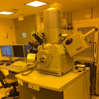
The Nova 200 is the KNI's highest-resolution field-emission gun (FEG) analytical scanning electron microscope (SEM), equipped with an immersion lens for imaging sub-10 nm features and energy dispersive spectroscopy (EDS) for compositional analysis. It is also outfitted with a gallium focused ion beam (Ga-FIB) column, which is currently not operational because the Nova 600 NanoLab and ORION NanoFab together meet the KNI's Ga-FIB demand; Ga-FIB could be reactivated on the Nova 200 in the future. See a full list of training and educational resources for this instrument below.
SEM Applications
- Ultra-High-Resolution Imaging (Immersion Mode aka UHR Mode)
- High-Resolution Imaging (Field-Free Mode aka Normal Mode)
- Secondary Electron (SE) imaging with an Everhart-Thornley Detector (ETD) & Through-the-Lens Detector (TLD)
- Backscattered Electron (BSE) imaging with a TLD
- Tungsten deposition via Gas Injection System (GIS)
- Automated imaging with RunScript program & AutoScript language
EDS Applications
- Spectrum acquisition for qualitative and quantitative compositional analysis
- Linescan acquisition for 1D spatial compositional analysis
- Map acquisition for 2D spatial compositional analysis
Resources
Equipment Data
SOPs & Manuals & SDS
- KNI Microscopy Policies
- Nova200 and EDS SOP, Manuals, SDS
- Nova NanoLab Operation Manual
- Bruker Quantax EDS Operation Manual
- Gas Injection Systems – Deposition of Tungsten (Technical Note)
- Gas Injection Systems – Delineation Etch for SiO2 (Technical Note)
- Gas Injection Systems – Selective Carbon Etching (Technical Note)
- Scripting – AutoScript Language Manual (year 2000 Technical Note: most complete)
- Scripting – RunScript Manual
Video Tutorials
- Getting Started | Basic SEM Alignment
- Astigmatism Correction (Details | On Right-Angle Features | Stigmator Alignment)
- Adjusting TLD Voltage to Capture SE vs. BSE Signal
- Bruker EDS ESPRIT 2 Software (Overview | Basic Spectrum Collection and ID | Spectrum Acquisiton | AutoID Verification | Object Mode (Multi-Point Analysis) | Line Profile Analysis)
Graphical Handouts
Presentations
- Scanning Electron Microscopy: Principles, Techniques & Applications
- Gallium Focused Ion Beam Microscopy: Principles, Techniques & Applications
Simulation Software
- CASINO Electron Beam Simulation Software – simulate e-beam/specimen interactions (very useful for EDS & WDS)
- The Stopping & Range of Ions in Matter (SRIM) – simulate i-beam/specimen interactions
Calibrate Measurements with NIST Standard
- The KNI has a NIST-traceable standard against which SEM measurements can be compared. See Slides 54-55 of the SEM Presentation for details. Ask staff for help finding and using the standard in the lab.
Sample Preparation
- Use the Carbon Evaporator to make non-conductive samples conductive by applying 2-10 nm of evaporated carbon.
- Use the O2/Ar Plasma Cleaner to remove hydrocarbons from the sample surface to avoid creating dark contamination spots on your features while imaging them.
Stubs for specimen mounting
- Stubs used for mounting specimens are considered a personal, consumable item in the KNI. There are some stubs at each Microscope which can be used by any KNI microscopy user. You can also buy your own stubs so that you can keep them clean and available to you. There are many stub geometries and configurations. If you chose to buy your own stubs, please show them to the staff microscopist prior to using them: some stubs including stubs with copper clips have large height differences and can only be used safely in specific operating conditions.
Guide to Choosing KNI SEMs & FIBs
Specifications
Manufacturer Specifications
- Nova 200 NanoLab Data Sheet (not all parameters apply to our instrument, see below for details specific to the KNI's Nova 200)
SEM Specifications
- Minimum Feature Size Resolved in Immersion Mode: ~5 nm
- Voltage Range: 0.2 to 30.0 kV
- Current Range: ~10 pA to 20 nA
- Apertures: 30 μm, 40 μm, 50 μm, 100 μm
- Eucentric Height: ~4.8 mm working distance (WD)
- Stage Range: ±25 mm X & Y travel, 50 mm Z travel, -12 to 58° tilt, 360° rotation
- ETD Grid Bias Range: -150 to 300 V
- TLD Bias Range: -100 to 150 V
- Ultimate Vacuum: 5e-6 mbar
Related Instrumentation in the KNI
Scanning Electron Microscopes (SEMs)
- Nova 600 NanoLab: SEM, Ga-FIB, GIS & Omniprobe
- Nova 200 NanoLab: SEM & EDS
- Sirion: SEM & EDS
- Quanta 200F: SEM, ESEM, Lithography & Probe Station
Focused Ion Beam (FIB) Systems
Sample Preparation for Microscopy
- Carbon Evaporator (Leica EM ACE600) to make samples conductive
- Oxygen & Argon Plasma Cleaner (Tergeo Plus ICP- & CCP-RIE) to remove hydrocarbons from surface
