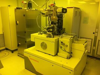
EBPG 5200: 100 kV Electron Beam Lithography: Difference between revisions
Jump to navigation
Jump to search
| Line 28: | Line 28: | ||
== Resources == | == Resources == | ||
===== SOPs & Troubleshooting ===== | ===== SOPs & Troubleshooting ===== | ||
* SOP Type ([https://caltech.box.com/s/ | * EBPG SOP Type ([https://caltech.box.com/s/qzhf1h1su3a1vadl6p76mg6tav49uisn Short Version] | [https://caltech.box.com/s/xwjdudqdl793gkc5kl71zez5nnc5y2xb Long Version]) | ||
* [https://caltech.box.com/s/ | * [https://caltech.box.com/s/1nmp75l3166vj9t1vwwpwu2zyfc4j6ol KNI SOP] | ||
* [https://caltech.box.com/s/1nmp75l3166vj9t1vwwpwu2zyfc4j6ol Other SOP1] | * [https://caltech.box.com/s/1nmp75l3166vj9t1vwwpwu2zyfc4j6ol Other SOP1] | ||
* [https://caltech.box.com/s/1nmp75l3166vj9t1vwwpwu2zyfc4j6ol Other SOP2] | * [https://caltech.box.com/s/1nmp75l3166vj9t1vwwpwu2zyfc4j6ol Other SOP2] | ||
Revision as of 17:34, 2 May 2019
|
Description
The Raith EBPG 5200 is a dedicated direct-write Electron Beam Pattern Generator that is used to pattern large areas by high resolution electron beam lithography. This instrument has substrate holders to handle 3" wafers, piece parts from a couple of mm to 3" diameter and up to 6.35mm thick, and 6" mask plates. This instrument can be outfitted with substrate holders to handle up to 200mm wafers. While this instrument can be set to operate at 20, 50, or 100 keV, it is normally set for 100 keV operation.
Opertional Applications
- Non-aligned electron beam lithography
- Aligned (AKA direct-write) electron beam lithography
Scientific / technical Applications
- Nanophotonics
- Nano-optics
- Waveguides
Resources
SOPs & Troubleshooting
- EBPG SOP Type (Short Version | Long Version)
- KNI SOP
- Other SOP1
- Other SOP2
- Troubleshooting Guide
Video Tutorials
Graphical Handouts
Presentations
Manufacturer Manuals
Specifications
Manufacturer Specifications
Specifications
- Voltage Range: 20, 50 or 100 kV
- Current Range: 50 pA - >200 nA
- Main Field size: Up to 1mm x 1mm
- Main Field resolution: 20 bit
- Maximum writing frequency: 100 MHz
- Aperture Sizes: 200um, 300um, 400um
- etc.
