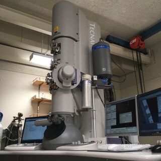
Tecnai TF-30: 300 kV TEM, STEM, EDS & HAADF: Difference between revisions
Jump to navigation
Jump to search
No edit summary |
|||
| Line 14: | Line 14: | ||
|RequestTraining = matthew.hunt@caltech.edu | |RequestTraining = matthew.hunt@caltech.edu | ||
|EmailList = kni-tf30 | |EmailList = kni-tf30 | ||
|EmailListName = | |EmailListName = TF-30 | ||
}} | }} | ||
== Description == | == Description == | ||
| Line 28: | Line 28: | ||
== Resources == | == Resources == | ||
===== SOPs & Troubleshooting ===== | ===== SOPs & Troubleshooting ===== | ||
* | * [https://caltech.box.com/s/v7oih7yv8yxai5ybkg8znplc54xc99if SOP Guide] | ||
* [https://caltech.box.com/s/b5h0v6s2ethshh2fs5o4eqwf7pe8sdwc Troubleshooting Guide] | |||
* [https://caltech.box.com/s/ | |||
===== Manufacturer Manuals ===== | ===== Manufacturer Manuals ===== | ||
* [https://caltech.box.com/s/og4309108q4k2jwhkaxqtpiujg2al5iu | * [https://caltech.box.com/s/og4309108q4k2jwhkaxqtpiujg2al5iu Tecnai TF-30 Manual (BROKEN)] | ||
===== Sample Preparation ===== | |||
* | * Sample preparation is a highly specific task related to each sample type and is therefore primarily the responsibility of the user to carry out. | ||
* | ** KNI staff can teach users how to create lamellae from a bulk specimen using an SEM/Ga-FIB system (see [https://caltech.box.com/s/3l3w507dxwosuya3nbxgk30tdqyp4qy9 SOP] and [https://www.youtube.com/playlist?list=PL7Lb5X_YIzOkg3wRe6A5a5b76fFxYyT3s YouTube playlist]) | ||
** The KNI also has a TEM sample preparation lab that is primarily used to make cross-section samples by traditional methods (i.e. glue together a stack, cut out 3 mm core, thin by polishing, dimple, then final polish with argo mill); inquire with staff for help with these tools | |||
===== Order Your Own Grids ===== | |||
* Grids used for mounting specimens are considered a personal, consumable item in the KNI. You are required to supply your own grids. | |||
* | |||
* | |||
===== Order Your Own | |||
* | |||
== Specifications == | == Specifications == | ||
===== Manufacturer Specifications ===== | ===== Manufacturer Specifications ===== | ||
* [https://caltech.box.com/s/ | * [https://caltech.box.com/s/e2mw7hh44g2hbcui5m3hnnqnlyunb8lf TF-30 Product Guide & Specifications] | ||
===== | ===== TEM & STEM Specifications ===== | ||
* 0. | * From FEI’s (now Thermo Fisher’s) Tecnai G<sup>2</sup> F30 Family | ||
* | * Voltage Range: 80-300 kV | ||
* | * Point resolution: 0.20 nm | ||
* Line resolution: 0.10 nm | |||
* | * STEM resolution: 0.17 nm | ||
* | * Information limit: 0.14 nm | ||
* | * Energy spread: 0.7 eV | ||
* Max alpha-tilt angle with double-tilt holder: ±40° | |||
* Max alpha-tilt angle with tomography holder: ±80° | |||
* Maximum diffraction angle: ±12° | |||
* Camera length: 35–2300 mm | |||
* EDS solid angle: 0.13 srad | |||
Revision as of 00:20, 6 May 2019
|
Description
The Tecnai TF-30 is a transmission electron microscope (TEM) that can also be operated in scanning transmission electron microscopy (STEM) mode, with a voltage range of 80 to 300 kV. Operation at 300 kV makes this the KNI's highest resolution TEM (see also the 200 kV Tecnai TF-20). The TF-30 is also equipped with a high-angle annular dark field (HAADF) detector for use in STEM mode, and an energy dispersive spectroscopy (EDS) detector for compositional analysis (in both TEM mode and, most usually, in STEM mode). The Serial EM program allows for automated collection of images at variable tilt angles for performing tomography. See a full list of training and educational resources for this instrument below.
Applications
- High-Resolution TEM (HRTEM) imaging without an objective aperture
- Bright Field (BF) & Dark Field (DF) imaging with an objective aperture
- Selected Area Electron Diffraction (SAED)
- STEM imaging with a High-Angle Annular Dark Field (HAADF) detector
- Energy Dispersive Spectroscopy (EDS) with Oxford INCA system
- Automatically capture tilt series of images for tomographic imaging
Resources
SOPs & Troubleshooting
Manufacturer Manuals
Sample Preparation
- Sample preparation is a highly specific task related to each sample type and is therefore primarily the responsibility of the user to carry out.
- KNI staff can teach users how to create lamellae from a bulk specimen using an SEM/Ga-FIB system (see SOP and YouTube playlist)
- The KNI also has a TEM sample preparation lab that is primarily used to make cross-section samples by traditional methods (i.e. glue together a stack, cut out 3 mm core, thin by polishing, dimple, then final polish with argo mill); inquire with staff for help with these tools
Order Your Own Grids
- Grids used for mounting specimens are considered a personal, consumable item in the KNI. You are required to supply your own grids.
Specifications
Manufacturer Specifications
TEM & STEM Specifications
- From FEI’s (now Thermo Fisher’s) Tecnai G2 F30 Family
- Voltage Range: 80-300 kV
- Point resolution: 0.20 nm
- Line resolution: 0.10 nm
- STEM resolution: 0.17 nm
- Information limit: 0.14 nm
- Energy spread: 0.7 eV
- Max alpha-tilt angle with double-tilt holder: ±40°
- Max alpha-tilt angle with tomography holder: ±80°
- Maximum diffraction angle: ±12°
- Camera length: 35–2300 mm
- EDS solid angle: 0.13 srad
