Nova 600 NanoLab: SEM, Ga-FIB, GIS & Omniprobe: Difference between revisions
Jump to navigation
Jump to search
| Line 24: | Line 24: | ||
* Backscattered Electron (BSE) imaging with a TLD | * Backscattered Electron (BSE) imaging with a TLD | ||
* Platinum deposition via Gas Injection System (GIS) | * Platinum deposition via Gas Injection System (GIS) | ||
* Automated imaging with RunScript program & AutoScript language | |||
===== Ga-FIB Applications ===== | ===== Ga-FIB Applications ===== | ||
Revision as of 00:37, 25 April 2019
|
Description
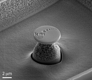
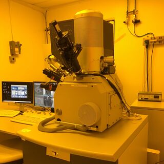
The Nova 600 is a "dual beam" system that combines a scanning electron microscope (SEM) with a gallium focused ion beam (Ga-FIB). It can be used to capture high quality images (with sub-10 nm resolution) and perform site-specific etching and material deposition (with sub-50 nm resolution). It is also equipped with an Omniprobe lift-out system for TEM lamella sample preparation. See a full list of training and educational resources for this instrument below.
SEM Applications
- Ultra-High-Resolution Imaging (Immersion Mode aka UHR Mode)
- High-Resolution Imaging (Field-Free Mode aka Normal Mode)
- Secondary Electron (SE) imaging with an Everhart-Thornley Detector (ETD) & Through-the-Lens Detector (TLD)
- Backscattered Electron (BSE) imaging with a TLD
- Platinum deposition via Gas Injection System (GIS)
- Automated imaging with RunScript program & AutoScript language
Ga-FIB Applications
- Directly etch patterns into material
- Cutting & Imaging Cross-Sections
- TEM Lamella Sample Preparation using an Omniprobe for Liftout
- Platinum & SiOx deposition via GIS
- Enhanced etch with XeF2 via GIS
- Automated patterning with RunScript program & AutoScript language
Resources
SOPs & Troubleshooting
- SEM SOPs (Short Version | Long Version)
- Ga-FIB SOPs (Short Version | Long Version)
- TEM Lamella Sample Preparation SOPs (Short Version | Long Version)
- Cutting & Imaging Cross-Sections SOP
- Troubleshooting Guide
Video Tutorials
- Getting Started | Basic SEM Alignment
- Astigmatism Correction (Details | On Right-Angle Features | Stigmator Alignment)
- Eucentric Height: What it means, When to use it & How to get there
- TEM Lamella Sample Prep (Playlist)
- Cutting & Imaging Cross-sections (Playlist)
- Milling Non-Conductive Samples using Charge Compensation
- Perfecting Ga-FIB Alignments
- Adjusting TLD Voltage to Capture SE vs. BSE Signal
Graphical Handouts
Presentations
- Scanning Electron Microscopy: Principles, Techniques & Applications
- Gallium Focused Ion Beam Microscopy: Principles, Techniques & Applications
Manufacturer Manuals
- Nova NanoLab Operation Manual
- Gas Injection Systems – Deposition of Platinum (Technical Note)
- Gas Injection Systems – Deposition of SiOx (Technical Note)
- Gas Injection Systems – Etching with IEE aka XeF2 Etch (Technical Note)
- Gas Injection Systems – Beam Chemistries Presentation
- Scripting – AutoScript Language Manual (year 2000 Technical Note: most complete)
- Scripting – AutoScript Language Manual (year 2005 Technical Note: less complete, still useful)
- Scripting – RunScript Manual
Simulation Software
- CASINO Electron Beam Simulation Software – simulate e-beam/specimen interactions
- The Stopping & Range of Ions in Matter (SRIM) – simulate i-beam/specimen interactions
Order Your Own Stubs
- Stubs used for mounting specimens are considered a personal, consumable item in the KNI. There are some old stubs at each SEM, yet you should buy your own so that you can keep them clean and available to you. There are many stub geometries and configurations, some of which will be right for you to purchase and keep with your other cleanroom items.
Specifications
Manufacturer Specifications
- Nova 600 NanoLab Data Sheet (not all parameters apply to our instrument, see below for details specific to the KNI's Nova 600)
SEM Specifications
- 0.5 to 30.0 kV
- Apertures: 10 mm, 15 mm, 20 mmm, 30 mm
- etc.
Ga-FIB Specifications
- 5.0 to 30.0 kV
- 10 pA - 20 nA
- etc.

