Nova 200 NanoLab: SEM & EDS
Jump to navigation
Jump to search
|
Description
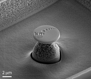
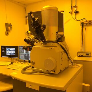
The Nova 200 is the KNI's highest-resolution analytical scanning electron microscope (SEM), equipped with an immersion-lens for imaging sub-10 nm features and both energy dispersive spectroscopy (EDS) and wavelength dispersive spectroscopy (WDS) detectors for compositional analysis. It is also outfitted with a gallium focused ion beam (Ga-FIB) column, which is currently not operational because the Nova 600 NanoLab and ORION NanoFab together meet the KNI's Ga-FIB demand; gallium could be reactivated on the Nova 200 the future. See a full list of training and educational resources for this instrument below.
SEM Applications
- Ultra-High-Resolution Imaging (Immersion Mode)
- High-Resolution Imaging (Field-Free Mode)
- Secondary Electron (SE) & Backscattered Electron (BSE) Imaging
- Everhart-Thornley Detector (ETD) & Through-the-Lens Detector (TLD)
- Tungsten deposition via Gas Injection System (GIS)
- Automated imaging with RunScript program & AutoScript language
Analytical Applications
- Compositional analysis with EDS (via x-ray detection)
- Compositional analysis with WDS (via x-ray detection)
Resources
SOPs & Troubleshooting
- SEM SOPs (Short Version | Long Version)
- Ga-FIB SOPs (Short Version | Long Version)
- TEM Lamella Sample Preparation SOPs (Short Version | Long Version)
- Cutting & Imaging Cross-Sections SOP
- Troubleshooting Guide
Video Tutorials
- Getting Started | Basic SEM Alignment
- Astigmatism Correction (Details | On Right-Angle Features | Stigmator Alignment)
- Eucentric Height: What it means, When to use it & How to get there
- Adjusting TLD Voltage to Capture SE vs. BSE Signal
Graphical Handouts
Presentations
Manufacturer Manuals
- Nova NanoLab Operation Manual
- Gas Injection Systems – Deposition of Platinum (Technical Note)
- Gas Injection Systems – Deposition of SiOx (Technical Note)
- Gas Injection Systems – Etching with IEE aka XeF2 Etch (Technical Note)
- Gas Injection Systems – Beam Chemistries Presentation
- Scripting – AutoScript Language Manual (year 2000 Technical Note: most complete)
- Scripting – AutoScript Language Manual (year 2005 Technical Note: less complete, still useful)
- Scripting – RunScript Manual
Specifications
Manufacturer Specifications
- Nova 600 NanoLab Data Sheet (not all parameters apply to our instrument, see below for details specific to the KNI's Nova 600)
Scanning Electron Microscope (SEM) Specifications
- 0.5 to 30.0 kV
- Apertures: 10 mm, 15 mm, 20 mmm, 30 mm
- etc.
Gallium Focused Ion Beam (Ga-FIB) Specifications
- 5.0 to 30.0 kV
- 10 pA - 20 nA
- etc.

